The End of the CPU Monopoly: History and Revolution of Logical Architectures in the Age of Artificial Intelligence
The end of CPU
The transition from general-purpose architectures to domain-specific accelerators is not merely an engineering optimization, but a capitalist strategy of accumulation. While commoditized CPU enabled limited margins and relatively open competition, specialized accelerators—through proprietary software ecosystems, technical lock-in, and layered patents—create barriers to entry that enable higher rent extraction.
The NVIDIA case is paradigmatic: its 85% market share does not stem from absolute technical superiority, but from the CUDA ecosystem—an example of digital enclosure where collectively accumulated technical knowledge (in universities, public labs) is captured and made proprietary through software interfaces.
CPU: Infrastructural Concentration and Systemic Dependence
Specialization accelerates the vertical concentration of computational power. While the CPU era saw relative distribution (multiple foundries, licensed ISAs like x86), the accelerator era brings extreme consolidation:
- Concentrated manufacturing (TSMC, Samsung for advanced nodes)
- Concentrated design (NVIDIA, Google, a few others)
- Proprietary software ecosystems that create structural dependencies
This concentration transforms compute from a relatively distributable resource into critical infrastructure controlled by oligopolies, with geopolitical implications that transcend pure market economics.
The collapse of Dennard scaling and the slowdown of Moore’s Law are not simply physical limits, but a valorization crisis in technological capitalism. When progress through miniaturization stalls, capital must find new frontiers of accumulation—hence the race toward specialization.
The Eclipse of CPU and the Stored-Program Architecture Paradigm
The semiconductor industry is undergoing an epochal transformation that redefines the very foundations of computing. After more than half a century of uncontested dominance by the stored-program architecture (improperly attributed to von Neumann) and the CPU as the universal processor, we now witness the rise of specialized architectures that challenge this monopoly: GPUs (Graphics Processing Units), TPUs (Tensor Processing Units), NPUs (Neural Processing Units), and LPUs (Language Processing Units). This revolution is not merely technical—it is a structural response to the physical and architectural limits that constrained computational progress over the last decades—and, as we will see, a new regime of accumulation in technological capitalism.
The Theoretical Foundations of CPU Logical Architecture: Von Neumann, Moore, and Dennard
CPU and Stored-Program Architecture: Eckert, Mauchly
The stored-program architecture that dominates modern computing has complex and politically contested origins. The actual inventors were J. Presper Eckert and John Mauchly at the Moore School of Electrical Engineering, University of Pennsylvania, who developed these concepts during and after work on ENIAC (Electronic Numerical Integrator and Computer), the world’s first digital computer.
As historically documented: “the attribution of the invention of the architecture to von Neumann is controversial, not least because Eckert and Mauchly had done much of the design work required and claim to have had the idea for stored programs long before discussing the ideas with von Neumann.”
John von Neumann, a mathematician and physicist consulting on the project, wrote in 1945 the “First Draft of a Report on the EDVAC”— a document that articulated, clarified, and systematically disseminated the principles of the architecture developed by Eckert and Mauchly. Widely circulated, this document solidified what would improperly become known as the “von Neumann architecture”—a paradigmatic example of how collective intellectual labor is often attributed to single figures occupying positions of higher academic prestige.
The architecture is based on distinct components: a central arithmetic unit, a control unit, unified memory for data and instructions (the revolutionary “stored-program” concept), and input/output mechanisms. It is this unified memory—where programs and data reside in the same address space—that constitutes both the power and the fundamental limit of the design.
The CPU Bottleneck
However, as critically identified by John Backus in his 1977 ACM Turing Award Lecture, this architecture—ironically known as the “von Neumann architecture” despite the contested attribution—contains a fundamental structural defect: the “von Neumann bottleneck” (the term itself reflects the now-entrenched misattribution in technical language). As Backus observed:
“Surely there must be a less primitive way of making big changes in the store than by pushing vast numbers of words back and forth through the von Neumann bottleneck. Not only is this tube a literal bottleneck for the data traffic of a problem, but, more importantly, it is an intellectual bottleneck that has kept us tied to word-at-a-time thinking.”
The bottleneck emerges from the physical separation between processor and memory, connected by a single shared bus. This forces the system to serialize access to instructions and data, creating a throughput limit regardless of the processor’s own speed. As highlighted in a Bernstein Research report (2016): “the speed of the architecture is limited by the speed at which the CPU can fetch instructions and data from memory.”
CPU: Moore’s Law and Dennard Scaling
For more than fifty years, the industry countered these architectural limits through technological progress. Moore’s Law, formulated by Gordon Moore in 1965, predicted the doubling of the number of transistors on an integrated chip roughly every two years. This was not a physical law, but an empirical observation that became a self-fulfilling roadmap for the industry.
In parallel, Dennard scaling, theorized by Robert Dennard in 1974, stated that as transistor dimensions shrink, power density remains constant—enabling higher frequencies and lower energy consumption. As documented by IEEE researchers: “Moore’s Law provided the commercial push to double the number of devices on an approximately two-year cadence, while Dennard’s scaling laws provided the physics to do it.”
However, in the early 2000s, both trends began to degrade. Dennard scaling broke down due to thermal dissipation and leakage issues, resulting in what has been called the “heat wall”—the thermal wall that stopped clock-frequency increases around the 65nm node. As noted in Daniel Etiemble’s paper “45-year CPU evolution” (LRI-CNRS): “CPU frequency limitation is correlated with the ‘heat wall’. According to the CMOS dynamic power dissipation equation, power dissipation is proportional to clock frequency.”
The Evolution of CPU Architectures: From CISC to RISC
CISC vs RISC
In the 1980s, processor architecture reached a fundamental crossroads. CISC (Complex Instruction Set Computer) processors—represented by Intel’s x86 architecture and the Motorola 68000 family— used complex instruction sets with the goal of reducing the number of instructions required to complete a task.
However, David Patterson at UC Berkeley and John Hennessy at Stanford proposed a radically different approach. In 1980, Patterson and colleague David Ditzel published “The Case for the Reduced Instruction Set Computer,” while Hennessy launched the MIPS project (Microprocessor without Interlocked Pipeline Stages) at Stanford.
The RISC approach, as articulated by Patterson and Hennessy, was based on counterintuitive principles:
- Reduced and simplified instruction set
- Fixed-length instructions
- Load/store architecture with register-to-register operations
- Deep pipelining to increase throughput
In 1982, Patterson’s team at Berkeley built and demonstrated the RISC-I processor which, with 44,000 transistors, outperformed a conventional CISC design using 100,000 transistors. As noted in ACM documentation: despite initial skepticism from many computer architects, the success of the MIPS and SPARC entrepreneurial efforts, the lower production costs of RISC designs, and further research advances led to wider RISC acceptance.
Patterson and Hennessy codified their shared insights in the foundational book “Computer Architecture: A Quantitative Approach” (1990), now in its seventh edition, influencing generations of engineers by introducing a quantitative, systematic framework for evaluating integrated architectures. For this work, the two researchers received the 2017 ACM A.M. Turing Award, the “Nobel Prize of computing.”
As Bill Gates emphasized in the award announcement: “the contributions of Patterson and Hennessy proved fundamental to the very foundations on which an entire industry flourished.”
The Dominance of x86 and the Intel–AMD CPU Duopoly
Despite RISC’s technical success, Intel’s x86 architecture maintained dominance in desktop and server markets due to non-technical factors: software compatibility, network effects, and barriers to entry created by patents and implementation complexity. As documented by Yatharth Sood in a 2020 analysis: “this dynamic market produced by strategy and circumstance has led to the creation of a less innovative space.”
The x86 architecture represents a duopoly between Intel and AMD, with significant barriers to entry. As the analysis highlights: “we have limited competition entering this space due to the investments that would be required and proprietary technology that can only be used under license.”
Internally, even modern x86 processors translate CISC instructions into RISC-like micro-operations, implicitly recognizing the superiority of the approach. This hybrid transformation adds further complexity and energy overhead.
CPU: The Multi-Core Transition and the Rise of Parallelism
CPU: From the Free Lunch to Dark Silicon
As documented by Antonio González in “Trends in Processor Architecture” (IEEE), until the mid-2000s, the industry enjoyed what was called the monoprocessor scaling “free lunch”: “for most applications, the best and cheapest way to increase performance was to wait for the next generation of processors.”
However, the collapse of Dennard scaling and the halt of frequency growth forced a transition toward multi-core architectures. As observed by Yale Patt (University of Texas): “we have already seen the end of Dennard scaling and its influence on microprocessor design.”
This transition introduced new complexities: as core counts rose, the phenomenon of “dark silicon” emerged—portions of the chip that must remain inactive due to thermal constraints. As highlighted in UCSD research: “with continued feature-size scaling, a growing fraction of the die must be ‘underutilized’ or ‘dark’ due to power constraints.”
The GPU Era: NVIDIA and the CUDA Revolution
From Graphics to AI: The Evolution of the GPU
Graphics Processing Units were born as specialized accelerators for rendering. However, their massively parallel architecture—thousands of simple cores optimized for vector math— made them ideally suited for workloads far beyond graphics.
The turning point came in 2006, when NVIDIA introduced CUDA (Compute Unified Device Architecture), a platform that extended GPUs from graphics rendering to general-purpose computing. As documented: “NVIDIA recognized the need for a simpler programming model for general-purpose GPU computing and launched CUDA in 2006.”
CUDA represented a fundamental paradigm shift: it allowed developers to program GPUs using familiar languages like C, C++ and Fortran, significantly lowering the barrier to entry. As noted by NVIDIA CEO Jensen Huang: “the world has a huge investment in non-AI software. CUDA-X and many open-source libraries and frameworks are where much of the magic happens.”
Tesla Architecture and Tensor Cores
NVIDIA’s Tesla architecture (2006) introduced the unified shader model, enabling GPU cores to run general-purpose computations efficiently. The first GPU to support CUDA was the GeForce 8800 GTX, with 128 unified shaders delivering unprecedented parallel compute.
The next evolution was pivotal for AI. In 2017, NVIDIA introduced Volta and the Tesla V100, described as “a seismic shift in GPU computing with the introduction of the first dedicated AI GPUs for datacenter HPC.” Tensor Cores, introduced with Volta, were specialized hardware units designed to accelerate mixed-precision tensor operations—crucial for deep learning.
As documented: “the flagship Tesla V100 GPU delivered up to 125 teraFLOPS of deep learning performance, marking a revolutionary step in AI hardware evolution.” Tensor Cores enabled mixed-precision training with FP16 compute while maintaining FP32 accuracy—unlocking unprecedented training speeds.
The CUDA Monopoly: Ecosystem as a Barrier
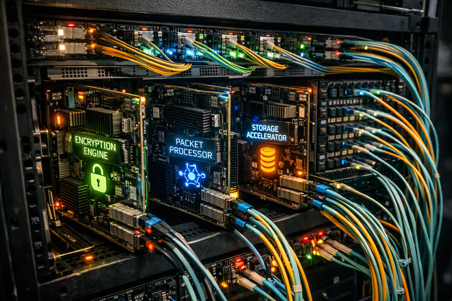
NVIDIA’s true power lies not only in hardware, but in the software ecosystem built around CUDA. As analyzed by Aidan Pak: “the root of NVIDIA’s GPU monopoly stems from its parallel computing platform CUDA, which enables NVIDIA GPUs to achieve higher compute utilization rates than competing architectures.”
NVIDIA developed essential specialized libraries:
- cuDNN for deep learning
- cuBLAS for basic linear algebra
- TensorRT for inference optimization
This ecosystem creates an effective lock-in: most AI engineers learn CUDA in university, and migrating to alternative platforms requires rewriting entire codebases. As of 2024, NVIDIA holds over 85% of the datacenter AI chip market, with “software-level” gross margins demonstrating the power of proprietary ecosystems— a perfect example of technological rent, where controlling the interface generates more value than hardware production itself.
The Memory Bottleneck in GPUs
Despite compute power, GPUs face significant limits linked to the memory hierarchy. As highlighted in research: “GPUs typically use existing GPGPU pipelines such as CUDA and OpenCL adapted for lower precision.” Data transfers between DRAM/HBM (High Bandwidth Memory) and compute units introduce hundreds of nanoseconds of latency per access, becoming a critical bottleneck for low-arithmetic-intensity inference workloads.
The shift from GDDR to HBM to HBM3e pushed bandwidth into the TB/s range, but the fundamental issue of memory–compute separation persists, rooted in the underlying von Neumann architecture.
Google TPU: The Systolic Array Revolution
CPU: The 2013 Compute Crisis
In 2013, Google faced an existential computational crisis. If every search request began using deep neural networks for three minutes of speech recognition, Google’s datacenters would have had to double. As the team recalled: “Google realized that the rapidly growing computational demands of neural networks could require doubling the number of datacenters it operates.”
This urgency led to an extraordinary decision for a software company: to design custom silicon. The goal: build an ASIC (Application-Specific Integrated Circuit) for a single task—running TensorFlow neural networks.
The project moved at exceptional speed: from initial discussions in late 2013 to the first TPUs deployed in datacenters in early 2015—just 15 months, dramatically shorter than the standard 3–5 years for production chips. That speed was possible precisely because the design was radically focused: neural inference and nothing else.
Systolic Array Architecture
The secret of TPU performance lies in the systolic array architecture, a concept originally outlined by H.T. Kung and Charles E. Leiserson in their 1978 paper “Systolic Arrays (for VLSI)”. As described in the paper: “In a systolic system, the function of a processor is analogous to that of the heart. Each processor regularly pumps data in and out, each time performing some short computations so that a steady flow of data is maintained in the network.”
Unlike CPU and GPUs, which constantly move data back and forth between memory and compute units, TPU systolic arrays let data flow through the chip like blood through a heart. As explained: “in a TPU’s systolic array, data flows through the chip. Each piece of data is used by multiple compute cells as it passes through, drastically minimizing memory accesses.”
Performance and a CISC Approach for AI
TPU v1 took a counterintuitive approach: a specialized CISC instruction set for neural inference. As explained: “typical RISC processors provide instructions for simple computations like multiplying or adding numbers. The TPU is more like CISC processors, which have more complex and varied instructions.”
The results were striking. As reported by Google: “the TPU delivered 15–30× higher performance and 30–80× higher performance-per-watt than contemporary CPU and GPUs.” These gains enabled many Google services to run state-of-the-art neural networks at scale and at viable cost.
Evolution: From v1 to Trillium and Ironwood
TPU v1 was inference-only. TPU v2 (2017) added training capability with floating-point support, high-bandwidth HBM (600 GB/s), and NVLink 2.0 for multi-accelerator communication. Google stated that TPU v2 chips were packaged in four-chip modules delivering 180 teraFLOPS, then assembled into 256-chip pods reaching 11.5 petaFLOPS.
Subsequent generations brought exponential improvements:
- TPU v4: Introduction of SparseCores for sparse operations
- TPU v5e: Up to 393 trillion int8 operations per second per chip
- Trillium (TPU v6): 67% better energy efficiency than v5e
- Ironwood (TPU v7): First TPU with native FP8 support, 4.6 petaFLOPS dense FP8 per chip, 192GB HBM3e with 7.4 TB/s bandwidth
As detailed in technical documentation: “each Ironwood chip provides 4.6 petaFLOPS of dense FP8 compute—slightly surpassing NVIDIA’s B200 at 4.5 petaFLOPS.”
The Ecosystem Problem
Despite superior performance, TPUs face a critical challenge: ecosystem. As analyzed: “the main problem for TPU adoption is the ecosystem. Nvidia’s CUDA is etched into the minds of most AI engineers. Google built its ecosystem internally but not externally, because it used TPUs only for internal workloads until relatively recently.”
TPUs rely on a mix of JAX and TensorFlow, while the industry gravitates toward CUDA and PyTorch. This fragmentation limits external adoption, confining TPUs largely to Google’s internal services and a subset of early adopters on Google Cloud.
Neural Processing Units (NPUs): AI at the Edge
Definition and NPU Architecture
Neural Processing Units (NPUs), also known as AI accelerators or deep learning processors, are specialized hardware accelerators designed to speed up artificial intelligence and machine learning applications, including artificial neural networks and computer vision. As defined by IBM: “an NPU is a specialized computer microprocessor designed to mimic the processing function of the human brain.”
Unlike general-purpose CPU or graphics-parallel GPUs, NPUs are designed specifically for neural operations: scalar, vector, and tensor computations that make up neural network layers. As documented: “NPUs use a computing architecture designed to simulate the neurons of the human brain to deliver high efficiency and high performance.”
The typical architecture of an NPU, as highlighted in academic literature on ScienceDirect, consists of:
- Massive arrays of Processing Elements (PE) for parallel operations
- Structured memory hierarchy
- Support for reduced precision (INT8, FP16) optimized for inference
- Data-reuse and computation-skipping techniques
As noted: “since DNNs require large amounts of data for both training and inference, memory bandwidth becomes crucial in NPU designs. Most NPUs use data-reuse techniques and skip unnecessary computations to address large off-/on-chip memory bandwidth.”
NPUs in Consumer Devices
Unlike GPUs and TPUs that dominate datacenters, NPUs found their primary niche in consumer and edge devices: smartphones, laptops, IoT. As documented by Synopsys: “the first neural network accelerators began to appear around 2014 when VGG16, a neural network model improving on AlexNet, became a widely used CNN architecture for visual classification tasks.”
Samsung Electronics launched the premium mobile application processor Exynos 9 (9820) with integrated NPU, claiming about 7× the computational power of the previous model. As highlighted: “while AI operations were previously performed via server connection, the Exynos 9 (9820) enables AI operations to occur within a mobile device for greater security.”
Intel integrated NPUs into Core Ultra processors, featuring Neural Compute Engines with hardware acceleration blocks for AI operations such as matrix multiplication and convolution. Their scalable multi-tile architecture supports up to 4,000 total MACs (Multiply-Accumulate) with 4MB near-compute memory.
Apple integrated the Neural Engine into M-series chips and iPhone processors, enabling extremely energy-efficient on-device AI. As noted: “NPUs are used in mobile devices such as Apple iPhone, AMD AI engines in Versal, Huawei and Google Pixel smartphones.”
Evolution of NPU Architectures
As documented by Synopsys on NPU evolution: “multiple advances in CNN architectures over the last eight years improved performance, efficiency, accuracy, and bandwidth at the cost of added hardware complexity. Hardware designed to maximize AlexNet, VGG16, or other early ImageNet-winning models would be inadequate today to efficiently run newer neural network models.”
Modern NPUs must support:
- Convolutional Neural Networks (CNNs) for computer vision
- Transformer networks for natural language processing
- Recurrent Neural Networks (RNNs) for sequential data
- Depthwise separable convolutions introduced by MobileNet
- Multiple activation functions (ReLU, GELU, Swish, etc.)
As highlighted: “the transformer neural network is a new type of deep learning architecture that originally gained traction due to its ability to perform natural language processing. Unlike RNNs, which process data serially and thus suffer from hardware bandwidth limits, transformers allow more parallelism.”
Performance and Comparison
Tests have shown that some NPU performance can be over 100× better than comparable GPUs at the same power consumption, thanks to domain-specific optimization. As noted by IBM: “capable of improving general operations (but more suitable for certain types of general tasks), when combined with CPU and GPUs, NPUs offer several valuable advantages over traditional systems.”
The challenge remains balancing specialization and flexibility: “the challenge for an NPU is to be optimized to accelerate math-intensive neural networks, area-efficient, and yet programmable enough to be future-proof when a new neural network technique or algorithm is published.”
Language Processing Units (LPUs): Groq and Deterministic Architecture
Genesis: Jonathan Ross and the Post-TPU
The story of Language Processing Units (LPUs) begins with Jonathan Ross, one of the original architects of Google’s TPU. In 2016, Ross left Google to found Groq, bringing accelerator design experience but with a radically different vision.
As documented: “Groq was founded in 2016 by a group of ex-Google engineers, led by Jonathan Ross, one of the designers of the Tensor Processing Unit (TPU), and Douglas Wightman, an entrepreneur and former Google X engineer.”
Ross’s key insight was that training and inference are fundamentally different workloads with divergent architectural requirements. As analyzed in detail: “the computational workload of an AI model changes drastically depending on whether it is learning (training) or thinking (inference). Training is a high-bandwidth, parallel task. Inference, instead, is sequential: you can’t predict word n+1 if you don’t have word n.”
The Von Neumann Bottleneck in LLM Inference
Large Language Models operate in a fundamentally sequential way during inference: they generate tokens one at a time in an autoregressive process. As explained: “in LLMs, processing is not parallel but serial: you can’t predict token n+1 without token n. That’s why parallel units like GPUs are not the highest-performing units for LLMs.”
GPUs, originally designed for graphics rendering with independent parallel operations, suffer structural inefficiencies in sequential inference. When a model generates text token-by-token, the GPU must continuously:
- Fetch weights from DRAM/HBM (hundreds of nanoseconds of latency)
- Load weights into compute units
- Execute computation
- Repeat for each layer, for each token
As critically highlighted: “both DRAM and HBM introduce significant latency on every weight fetch—hundreds of nanoseconds per access. This works for high-batch training where temporal locality is predictable and arithmetic intensity is high, but inference executes layers sequentially with far lower arithmetic intensity, exposing the latency penalty incurred by DRAM/HBM.”
Tensor Streaming Processor (TSP) Architecture
Groq’s answer is the Tensor Streaming Processor (TSP), later rebranded as the LPU, built on four principles:
1. Software-First: Inverting the Paradigm
Unlike traditional processors where the compiler is subordinate to hardware, Groq flips the relationship. The LPU is deliberately “dumb”: no branch predictor, no cache controller, no out-of-order execution. It is a massive array of arithmetic units that does exactly what it’s told, when it’s told. The compiler takes total control of execution.
2. SRAM at the Center: Eliminating Memory Latency
Instead of DRAM or HBM, the LPU integrates hundreds of megabytes of on-chip SRAM as primary weight storage. Result: drastically reduced access latency. Reading from DRAM consumes about 200× more energy than a multiply-accumulate—eliminating these accesses radically changes efficiency.
3. Determinism: Total Static Scheduling
The LPU eliminates all sources of non-determinism (interrupts, cache misses, context switches). The compiler can statically schedule every instruction and predict exactly when data will arrive. This enables optimizations impossible on traditional architectures.
4. A Programmable Assembly-Line Architecture
The LPU uses data “conveyor belts” that move instructions between functional units. Each unit receives instructions specifying where to take inputs, which function to execute, and where to place outputs—fully software-controlled, without hardware synchronization.
Performance: Beyond 1,600 Tokens per Second
The results are striking. Groq demonstrated text generation above 1,600 tokens per second—orders of magnitude faster than standard GPU implementations. Public demos showed models responding with instant blocks of text, generated faster than the human eye can read—no more ChatGPT-style “stuttering.”
For massive models like Kimi K2 (trillion parameters), the LPU architecture enables real-time token generation through optimized tensor parallelism. The LPU Inference Engine can auto-compile LLMs over 50B parameters with near-instant latency.
The secret: near-100% compute utilization, versus often-low GPU utilization during inference. The critical metric is not “cost per chip” but “cost per generated token”—and here, LPU energy efficiency changes the economics of AI inference.
Plesiosynchronous Multi-Chip Architecture
To scale beyond a single chip, Groq uses a plesiosynchronous chip-to-chip protocol that cancels natural clock drift and aligns hundreds of LPUs to act like a single core. As explained: “the SW compiler can therefore predict exactly when data will arrive, so developers can reason about timing. Periodic software sync adjusts for crystal-based drift, enabling not only compute scheduling but also network scheduling.”
A node is formed by 8 TSP devices in a chassis, each with 11 pins: 7 pins connect each TSP to the other 7 TSPs in the node, while the remaining 4 pins form a global link. The 32 total global links together form a high-radix virtual router with 32 ports.
Trade-offs and Limits
The LPU architecture comes with significant trade-offs:
- High upfront cost: hundreds of chips may be needed for a single large model, with higher initial CapEx than traditional GPU servers
- Extreme specialization: excels at sequential inference but struggles with dynamic compute patterns, conditional execution, sparse matrices
- Limited ecosystem: like TPUs, faces adoption challenges outside a proprietary ecosystem
However, efficiency per generated token—the metric that matters for inference providers—is dramatically higher. Energy consumed per token is significantly lower thanks to near-total compute utilization.
The NVIDIA Acquisition (2025)
In December 2025, NVIDIA announced an agreement to acquire assets from Groq for about $20 billion—a record for NVIDIA. As documented: “Groq described this as a non-exclusive licensing deal. As part of the agreement, Groq founder Ross and Groq president Sunny Madra will join NVIDIA.”
This acquisition signals a deep recognition: determinism is the destiny of future AI speed, and brute force is meaningless without the deterministic architecture that Groq pioneered to use it effectively.
Critical Analysis: The Political Economy of Specialized Architectures
Power Concentration and Technological Lock-In
The revolution of specialized architectures is not a neutral process driven solely by technical innovation, but a battlefield for control over computational infrastructure. The transition from general-purpose CPU to domain-specific accelerators has paradoxically increased the concentration of industrial power.
NVIDIA holds over 85% of the datacenter AI market not through absolute technical superiority, but through the CUDA ecosystem—an archetypal case of proprietary lock-in. Migrating away from CUDA requires massive code rewrites, staff retraining, and giving up decades of optimization. Google, even with TPU technology that is technically superior in many benchmarks, cannot dislodge this monopoly precisely due to ecosystem inertia.
Specialization turns AI compute from a general commodity into a differentiated service with significant pricing power. NVIDIA’s “software-level” gross margins show how specialized hardware enables higher rent extraction. This dynamic creates infrastructural dependence: companies building AI services depend on a handful of accelerator suppliers, creating barriers to entry that favor hyperscalers and incumbents.
Open Source: Necessary but Insufficient Resistance?
Projects like RISC-V represent critical attempts to build “technological commons” against privatization. But the dialectic is complex: an open ISA is necessary but not sufficient when software ecosystems and manufacturing capacity remain concentrated.
SPARC was open-sourced but failed; RISC-V gains traction mainly in embedded/IoT, not in the lucrative AI datacenter markets. Openness at the architectural level does not guarantee democratization when the upper layers of the stack remain proprietary—optimized compilers, libraries, toolchains require investments only a few actors can sustain.
Energy Sustainability: From Dennard to Dark Silicon
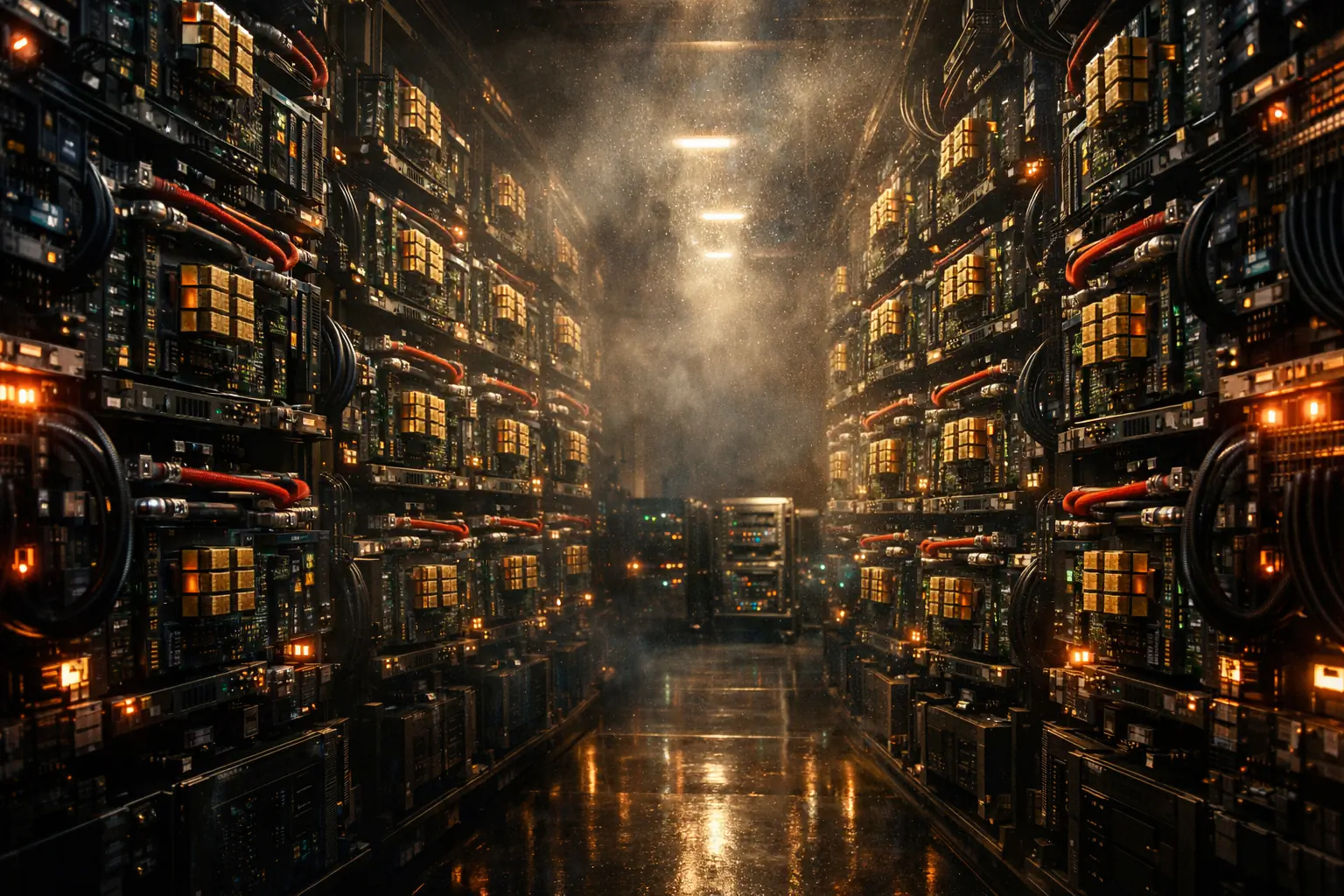
The shift toward accelerators was partly driven by real energy constraints—Dennard scaling collapse made continued CPU frequency scaling unsustainable. However, modern AI accelerators consume hundreds of watts per chip (TPU v7: 600W, NVIDIA H100: 700W), creating new cooling and sustainability challenges.
Dark silicon—growing portions of the die that must remain inactive due to thermal limits—is a fundamental physical constraint that even specialization cannot overcome indefinitely. Concentrating compute in centralized hyperscale datacenters amplifies environmental impact, despite efficiency gains per operation.
Geopolitics: Semiconductors as Strategic Weapons
Specialization has intensified the geopolitical dimension of semiconductors. US export controls on advanced NVIDIA GPUs to China show how AI accelerators are now strategic assets, not merely commercial goods.
Training advanced AI models requires access to clusters of thousands of accelerators, creating geopolitical dependencies that transcend traditional supply chains. Concentrating advanced manufacturing in TSMC (Taiwan) for cutting-edge GPU/TPU production and Samsung for NPU creates geopolitical single points of failure that governments try to mitigate through reshoring and industrial subsidies— but technological complexity makes concentration almost inevitable.
The Paradox of Specialization and the Crisis of CPU Generality
The revolution of specialized architectures presents a fundamental paradox that reflects deeper contradictions in technological capitalism: specialization increases efficiency for target workloads but reduces flexibility, increases fragmentation, and above all concentrates infrastructural control.
As researchers observed: “for general purpose computing, there is really nothing more powerful than the von Neumann [stored-program] architecture.” But that generality—historically enabling a relative democratization of software innovation—becomes economically unsustainable in the post-Dennard era. Technological capital must find new frontiers of valorization when pure miniaturized scaling stalls.
Returning to the Framework: Three Concluding Dynamics
1. From Commoditization to Rentierization
The CPU → specialized accelerator transition reverses the historical trajectory of semiconductor commoditization. While x86 processors, even under duopoly, saw margins compressed by relative interchangeability, AI accelerators enable “software-level” margins (NVIDIA) through ecosystem lock-in.
This represents a new phase of accumulation where value derives not primarily from hardware production, but from controlling software layers (CUDA, TensorFlow, JAX) that mediate access to hardware. It is a form of technological rent: whoever controls the interface controls the value flow, regardless of absolute technical superiority.
2. Concentration as a Systemic Necessity
The growing complexity of the tech stack—from chip design to advanced foundries (EUV lithography) to software ecosystems— makes concentration not merely a market outcome but a systemic necessity. Only a few actors can sustain the multi-billion-dollar investments required.
This concentration creates:
- Critical infrastructural dependencies: entire sectors depend on single suppliers (TSMC for advanced manufacturing, NVIDIA for AI training)
- Geopolitical asymmetries: control over advanced semiconductors becomes state power leverage (US export controls → China)
- Insurmountable barriers for distributed, bottom-up innovation
3. The Open Source Dialectic: Insufficient Resistance?
Projects like RISC-V are critical attempts to build “technological commons” resisting privatization. But the dialectic is complex: an open ISA is necessary but not sufficient when the software ecosystem (optimized compilers, libraries, toolchains) and manufacturing capacity remain concentrated.
As we’ve seen, SPARC was open-source but failed; RISC-V gains traction mainly in embedded/IoT, not in lucrative AI datacenter markets. Openness at the architectural level does not guarantee democratization when the upper layers of the stack remain proprietary.
Heterogeneity and Beyond Von Neumann CPU Logic
We are witnessing the rise of heterogeneous systems combining CPU, GPUs, TPU/NPU, and potentially LPUs. As documented by imec: “putting complex memory hierarchies, multicore architectures, and domain-specific compute accelerators (xPU) on a single system-on-chip has become a way to overcome scaling walls.”
This heterogeneity introduces orchestration, memory coherence, and programming complexity that may limit theoretical gains. More radical approaches like analog in-memory computing (IBM phase-change memory, Mythic AI) aim to overcome the von Neumann bottleneck by integrating memory and computation— but face maturity challenges and limited precision.
The Role of Open Source and Open Standards
RISC-V and projects like OpenCAPI for memory coherence represent critical efforts to democratize architectural innovation and reduce proprietary lock-in. As highlighted: “RISC-V from the University of California, Berkeley is the fifth version of the Berkeley RISC family of CPU architectures and is currently gaining great attention. It is generally accepted that this interest is due to the fact that the instruction set architecture (ISA) of RISC-V is Open Source, allowing its unrestricted use.”
However, history shows that open standards do not automatically guarantee market success—they require mature software ecosystems, complete toolchains, and critical mass of industrial adoption.
The rise of domain-specific architectures for AI raises the question: will we see similar specialization for other compute domains? Database processing units? Blockchain accelerators? Quantum-classical hybrid processors?
As Yale Patt critically observed: “there is no vacuum when it comes to microprocessor hype. Dark silicon, quantum computers, approximate computing all rushed in to fill the void.”
The fundamental challenge remains: balancing specialization for efficiency with flexibility for evolvability. As researchers put it: “the challenge for an NPU is to be optimized to accelerate math-intensive neural networks, area-efficient, and yet programmable enough to be future-proof when a new neural network technique or algorithm is published.”
Not Just CPU: A New Division of Computational Labor
What emerges is an increasingly sophisticated division of computational labor:
- CPU: Control flow, orchestration, irregular workloads
- GPU: AI training, compute-intensive parallelism, graphics
- TPU: Large-scale training, dense tensor operations
- NPU: Edge inference, extreme energy efficiency
- LPU: Ultra-low-latency inference, sequential generation
This division reflects the recognition that “one size fits all” became economically unsustainable in the post-Dennard era. As highlighted: “the traditional approach is not the best choice for some applications because it does not address key bottlenecks that exist in these workloads.”
The open question is whether this architectural fragmentation will create a richer, more innovative ecosystem, or whether it will further consolidate power in the hands of a few incumbents capable of sustaining ecosystems across multiple specialized architectures.
Power structures embedded in computational architectures:
- Mapping proprietary control: Systematic analysis of patents, licenses, and ecosystem dependencies in AI accelerators
- Alternative political economies: Case studies such as RISC-V, open-hardware projects, “sovereign compute” initiatives
- Material sustainability: Full lifecycle assessment (materials extraction → energy use → e-waste) of specialized architectures
- Democratic governance: Proposals for regulating critical compute infrastructure as public utilities
The Battlefield of Cognitive Infrastructure
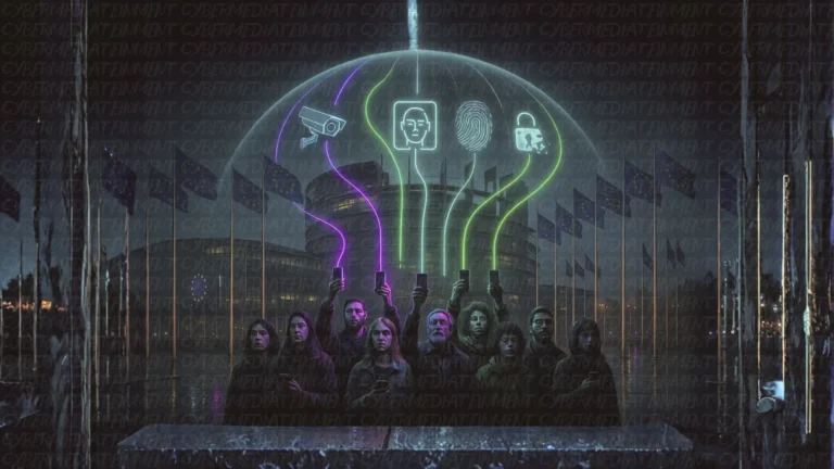
The architecture revolution is not inevitable technical progress, but a battlefield where it is decided who will control the cognitive infrastructure of the 21st century. The apparent “neutrality” of architectural choices hides deep political choices: who can innovate, who depends on whom, which computational futures are possible.
The extreme concentration we documented—NVIDIA with 85% of the datacenter AI market, advanced manufacturing in two foundries, proprietary ecosystems capturing decades of public research— is not inevitable. It is the result of choices: policy choices (patents, unblocked acquisitions), investment choices (public funding in basic research, private capture through proprietary interfaces), architectural choices (open standards vs closed).
As we saw with Eckert and Mauchly—the true inventors of the stored-program architecture who lost credit to von Neumann— the history of technology is also a history of appropriating collective intellectual labor. What we call the “von Neumann architecture” was developed by teams, spread through documents, implemented in publicly funded university projects. But it was privatized through patents, proprietary ecosystems, and manufacturing concentration.
The same dynamic repeats today with AI accelerators built on decades of public research in neural networks, linear algebra, and computer architecture— but captured through CUDA, proprietary TPUs, and ecosystem barriers that exclude bottom-up innovation.
Decoding these dynamics is a prerequisite for resisting—and possibly reclaiming—spaces of technological autonomy. Technology is not neutral. Architectures embed political choices. Our task is to make them visible—and contestable.
Decode. Resist. Reclaim.
Sources (external links)
- First Draft of a Report on the EDVAC — John von Neumann (1945)
- Can Programming Be Liberated from the von Neumann Style? — John Backus (CACM, 1978)
- Design of Ion-Implanted MOSFET’s with Very Small Physical Dimensions — R. H. Dennard et al. (1974)
- Dark Silicon and the End of Multicore Scaling — Esmaeilzadeh et al. (ISCA, 2011)
- CUDA Programming Guide (Introduction: CUDA in 2006) — NVIDIA Docs
- TensorFlow: A System for Large-Scale Machine Learning — Abadi et al. (OSDI, 2016)
- In-Datacenter Performance Analysis of a TPU — Jouppi et al. (2017)
- Systolic Arrays (for VLSI) — H. T. Kung & C. E. Leiserson (1978)
- Turing Award 2017 (Patterson & Hennessy) — ACM
- RISC-V (open standard, specs) — RISC-V International
- Nvidia, licensing deal + hires from Groq (December 24, 2025) — Reuters
SEO Keyword: machine learning